Introduction to the Winbond W29N01HVBINA NAND Flash Memory
The Winbond W29N01HVBINA represents a cutting-edge solution in the realm of non-volatile memory technologies, designed to cater to a wide range of digital storage requirements. This NAND Flash memory chip is built using SLC (Single-Level Cell) NAND technology, which provides a perfect blend of performance, reliability, and endurance. It offers a substantial storage capacity of 1Gb (128M x 8), making it an excellent choice for applications requiring high-density data storage. The W29N01HVBINA operates within a voltage supply range of 2.7V to 3.6V and is designed for surface mount technology, making it versatile for various electronic devices.

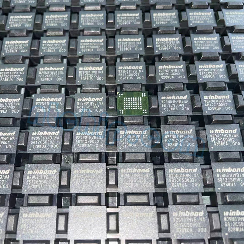
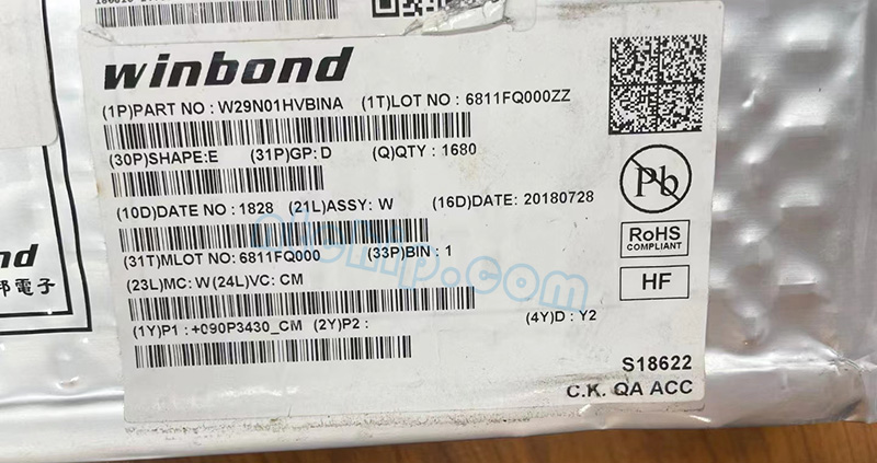
Winbond W29N01HVBINA Front and Back
Winbond is the manufacturer of the W29N01HVBINA, which is available in stock at Nantian. The reference price for W29N01HVBINA can be found by referring to Winbond or Nantian's listings. For detailed parameters and understanding its functionality, you can refer to the W29N01HVBINA datasheet PDF and pin diagram description that are available for download.
The W29N01HVBINA has a wide range of applications as outlined in DSP Datasheet PDF. To further understand how it works, you can find usage methods along with circuit diagrams within these resources. For comprehensive electronics tutorials on using this component, these documents should prove highly beneficial.

All relevant information including datasheets, pin diagrams, circuit diagrams and tutorials related to W29N01HVBINA could be downloaded from Nantian's platform.
Key Features
Memory Type: Non-Volatile, ensuring data is preserved even without power.
Memory Format: FLASH - employing NAND technology for efficient storage.
Technology: FLASH - NAND (SLC), offering superior reliability and faster write cycles.
Memory Size: 1Gb (128M x 8), providing ample space for data storage in a compact form factor.
Write Cycle Time - Word, Page: 25ns, enabling quick data writing and efficient performance.
Access Time: 25ns, allowing for rapid data retrieval.
Memory Interface: Parallel, facilitating easy integration into a wide array of system architectures.
Voltage - Supply: 2.7 V ~ 3.6 V, offering compatibility with a broad spectrum of electronic devices.
Operating Temperature: -40°C ~ 85°C (TA), ensuring stable operation under extreme conditions.
Mounting Type: Surface Mount, supporting modern, compact PCB designs.
Package / Case: 63-VFBGA, utilizing a small form factor for space-sensitive applications.
Supplier Device Package: 63-VFBGA (9x11), providing a standardized package for easy implementation.
Technical Specifications and Performance
The W29N01HVBINA flash memory chip is engineered with a parallel interface to ensure seamless communication with microcontrollers and processors.
Its Single-Level Cell (SLC) NAND technology not only enhances the reliability of the storage but also significantly increases the lifespan of the memory chip compared to multi-level cell (MLC) solutions.
The device’s quick write cycle and access times facilitate efficient data management and retrieval, making it suitable for high-performance computing environments.
Designed to operate in a wide range of temperatures, this memory chip is an ideal choice for applications exposed to environmental variations.
The compact 63-VFBGA package allows for a minimal footprint on PCBs, optimizing space for other critical components.
Applications and Integration
The versatility and high performance of the Winbond W29N01HVBINA make it an ideal memory solution for a diverse array of applications, including but not limited to, embedded systems, IoT devices, high-end computing platforms, and digital storage media. Its robust design and large storage capacity enable it to handle the rigorous demands of modern electronics, offering developers and manufacturers a reliable and efficient data storage option. The memory chip's compatibility with a wide voltage range and its ability to operate under extreme temperatures further broaden its applicability in various industrial, automotive, and consumer electronic products. With its parallel interface, the W29N01HVBINA can be easily integrated into existing designs, facilitating the development of advanced digital solutions.