In precision instrumentation design, industrial control, and electronic weighing applications, engineers often face a difficult trade-off: pursuing high-voltage power supply, achieving ultimate DC accuracy, or maintaining ultra-low noise?
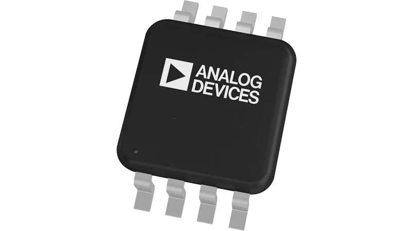
Today, we introduce the ADA4522-2ARMZ (the MSOP-8 packaged version of the ADA4522-2), a universal operational amplifier from Analog Devices (ADI) that shatters this compromise. This high-voltage op amp combines a 55V wide supply range, zero-drift architecture, integrated EMI filtering, and ultralow noise performance.
This article provides a comprehensive breakdown of the chip's technical specifications, application use cases, and crucial design considerations.
SHOP ADA4522-2ARMZ NOW
1. Key Parameter Breakdown: ADA4522-2ARMZ Specifications
In precision circuit design, simply knowing a component is "high-performance" is insufficient; we need concrete data to ensure sufficient design margin. The ADA4522-2ARMZ flawlessly integrates a 55V operating voltage with an extreme zero-drift architecture within a tiny MSOP-8 package. For applications demanding high dynamic range and low noise—such as industrial process control or precision current sensing—its 5.8 nV/sqrtHz noise density and 22 nV/C ultralow temperature drift stand as its most significant technical differentiators. Below are the most critical electrical characteristics for device selection:
| Key Parameter | Typical Value/Range | Unit | Notes |
|---|
| Supply Voltage | 4.5 to 55 | V | Supports single or dual supply (+-2.25 V to +-27.5 V) |
| Input Offset Voltage (VOS) | 5 (Max) | uV | Achieves high DC precision via chopping technology** |
| Offset Voltage Drift | 22 (Max) | nV/C | Ideal for the extended industrial temperature range (-40C to +125C) |
| Voltage Noise Density | 5.8 | nV/sqrtHz | At 1 kHz, AV = 100 |
| Noise (0.1 Hz to 10 Hz) | 117 | nV p-p | Excellent low-frequency noise performance |
| Input Bias Current (IB) | 50 | pA | Typical, suitable for high-impedance sensors |
| Gain Bandwidth Product (GBP) | 2.7 | MHz | At AV = 100 |
| Unity-Gain Crossover | 3.0 | MHz | Typical |
| EMI Rejection Ratio (EMIRR) | 80 | dB | At 900 MHz, due to integrated** EMI filters** |
| Package Type | 8-Lead MSOP | - | "ARMZ" suffix denotes the small MSOP package |
| Operating Temperature Range | -40 to +125 | C | Extended industrial range |
2. Internal Architecture: How the ADA4522-2 Achieves Zero Drift
Understanding the amplifier's internal operating principle is key to maximizing its performance.
Chopping Architecture: The ADA4522-2 uses chopping networks (CHOP_IN and CHOP_OUT) at the input and output, operating at 4.8 MHz. This technique modulates low-frequency errors (such as offset and 1/f noise) to a higher frequency, effectively removing them from the baseband signal.
Ripple Correction Loop: To mitigate artifacts introduced by the chopping process, the chip incorporates an internal offset and ripple correction loop running at 800 kHz, significantly reducing switching noise.
Robust Input Protection: The input stage includes series resistors, common-mode/differential capacitors, and back-to-back diodes. This not only filters EMI but also protects the internal circuitry from differential voltage transients up to +-5V and Electrostatic Discharge (ESD) events.
3. Core Highlights: Why Choose the ADA4522-2?
The ADA4522-2 is the dual-channel version within the ADA4522 family, specifically engineered for maximum total accuracy under varying time, temperature, and voltage conditions.
Wide Voltage Range and Power Flexibility:
High Voltage Operation: It supports a single supply from 4.5 V to 55 V, or a dual supply from +-2.25 V to +-27.5 V.
Versatility: This makes it an ideal choice for standard 5V, 10V, 12V, and 30V single-supply systems, as well as traditional +-5V, +-15V, and even higher industrial dual-supply systems.
Ultimate DC Accuracy (Zero Drift):
The ADA4522-2 utilizes chopping technology to eliminate 1/f noise and achieve extremely low error.
Low Offset Voltage (VOS): A maximum of only 5 uV.
Ultra-Low Drift: Maximum offset voltage drift is 22 nV/C. This ensures that the error remains negligible across the wide industrial temperature range of -40C to +125C.
High Open-Loop Gain: This makes the device perfectly suited for amplifying tiny input signals.
Ultra-Low Noise Performance:
While many zero-drift op amps typically exhibit high broadband noise, the ADA4522-2 is an exception.
Voltage Noise Density: A typical value of only 5.8 nV/sqrtHz (at 1 kHz).
1/f Noise (0.1 Hz to 10 Hz): Typically 117 nV p-p.
Application Advantage: This low-noise characteristic makes it the ideal choice for high-precision measurement applications.
Enhanced EMI Immunity:
Integrated EMI Filters: The input stage features integrated EMI filtering and clamping circuits that effectively suppress electromagnetic interference (EMI).
EMIRR: The EMI Rejection Ratio (EMIRR) is a robust 80 dB at 900 MHz. This is crucial for maintaining signal integrity in modern industrial settings saturated with wireless signals (Wi-Fi, Bluetooth, cellular).
4. Key Application Use Cases
Leveraging its "zero drift" and "high voltage" capabilities, the ADA4522-2 excels in the following demanding areas:
Weigh Scales and Load Cells: The ADA4522-2's ultra-low offset and drift make it an ideal front-end amplifier for handling the extremely weak signals from load cell and bridge transducers. It provides the high gain necessary to accurately process microvolt-level signals from a Wheatstone bridge, unaffected by temperature variations.
Precision Low-Side Current Sensing: In motor control or power management, the low offset voltage of the ADA4522-2 ensures absolute accuracy even when amplifying the microvolt drops generated by low currents. This is critical for precision low-side sensing.
Automotive and Industrial Sensors: With AEC-Q100 qualification (for specific models), the device is suitable for demanding automotive sensor applications, including on-board chargers (OBC) and Battery Management Systems (BMS).
5. ADA4522-2ARMZ Pin Configuration

ADA4522-2ARMZ-Pin-configuration
The ADA4522-2ARMZ utilizes the industry-standard, space-saving 8-Lead MSOP package (RM-8). As a dual-channel operational amplifier, this configuration provides two independent and fully functional precision amplifiers, making it ideal for high-density integration applications. This small footprint allows the chip to be easily incorporated into space-constrained industrial modules and portable instrumentation.
The 8-pin arrangement follows the classic dual op amp layout, simplifying design and routing for engineers. Pins 2 and 3 (INA-/INA+) form the input stage for the first amplifier, while Pins 5 and 6 (INB+/INB-) serve as the inputs for the second channel. Pins 1 (OUTA) and Pins 7 (OUTB) are the respective outputs. Pins 8 (V_S+) and Pins 4 (V_S-) provide the wide 55V power supply; in common single-supply operation, Pin 4 (V_S-) is typically connected to system ground (GND).
6. Manufacturer Spotlight: Analog Devices (ADI)
When discussing highly precise and reliable chips like the ADA4522-2, the manufacturer's pedigree is paramount. Analog Devices, Inc. (ADI), founded in 1965, is a global leader in high-performance analog, mixed-signal, and Digital Signal Processing (DSP) integrated circuits.
ADI's core mission is to act as the bridge between the physical and digital worlds. They specialize in converting real-world phenomena (such as light, sound, temperature, and pressure) into electronic signals for precise measurement, conditioning, and processing. ADI maintains a commanding presence in key component markets, including Analog-to-Digital Converters (ADCs), Digital-to-Analog Converters (DACs), and high-performance operational amplifiers like the ADA4522 family. Their high-quality, high-accuracy solutions are widely deployed across high-reliability sectors such as Industrial Automation (Industry 4.0), Automotive Electronics, communications infrastructure, healthcare, and precision instrumentation.
7. Summary
The ADA4522-2ARMZ is an exceptionally powerful operational amplifier that resolves the traditional design conflict between "high voltage" and "high precision." Whether used in high-accuracy weighing scales, complex industrial process control systems, or automotive battery management systems (BMS), it consistently delivers extremely stable, low-noise signal conditioning capabilities, making it the top choice for today's most challenging precision amplifier applications.
FAQ
What is the key advantage of its "Zero-Drift" architecture?
It uses Chopping technology to minimize maximum input offset voltage to 5 uV, with extremely low drift (max 22 nV/C), ensuring high accuracy over temperature.
What is the maximum supply voltage it supports?
It supports up to 55 V single supply or +-27.5 V dual supply, making it versatile for high-voltage industrial systems.
How strong is its EMI immunity?
Very strong. It has integrated EMI filters and clamping circuits at the input, achieving an EMIRR of 80 dB at 900 MHz to suppress electromagnetic interference.
What are the noise performance specifications?
Ultra-low voltage noise density: typically 5.8 nV/sqrtHz (at 1 kHz), and very low 0.1 Hz to 10 Hz noise (117 nV p-p).
What is its Gain Bandwidth Product (GBW)?
Typically 3 MHz (unity-gain crossover), suitable for applications where speed is moderate but DC precision is paramount.


