Introduction
In the dynamic world of semiconductor technology, understanding the nuances and functionalities of different components is crucial for anyone keen on electronics. Two such critical components are NMOS (N-channel Metal-Oxide-Semiconductor) and PMOS (P-channel Metal-Oxide-Semiconductor) transistors. These transistors, though similar in their fundamental purpose, exhibit distinct characteristics and applications. This blog aims to elucidate the differences between NMOS and PMOS transistors, shedding light on their individual strengths and how they complement each other in modern electronic devices.
What is NMOS?
NMOS, or N-type Metal Oxide Semiconductor, is a type of MOSFET (Metal Oxide Semiconductor Field Effect Transistor) where the majority carriers are electrons. The name derives from the use of n-type semiconductors as the source and drain regions. In an NMOS transistor, when a positive voltage is applied to the gate terminal relative to the source terminal, it creates an electric field that attracts electrons towards the gate. This forms a conductive channel between the source and drain terminals allowing current to flow through.
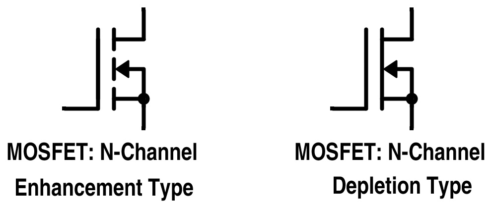
Enhancement(left) and Depletion(right) NMOS Symbol
NMOS Advantages Over PMOS
The main advantages of NMOS transistors include their speed and size. They switch faster than PMOS transistors due to electron mobility being higher than hole mobility, which makes them more suitable for high-speed applications. Additionally, because they can be made smaller than equivalent PMOS devices (due again to electron properties), they allow for denser and more compact integrated circuits.
NMOS, or N-type Metal Oxide Semiconductor, is a type of MOSFET (Metal Oxide Semiconductor Field Effect Transistor) where the majority carriers are electrons. The name derives from the use of n-type semiconductors as the source and drain regions. In an NMOS transistor, when a positive voltage is applied to the gate terminal relative to the source terminal, it creates an electric field that attracts electrons towards the gate. This forms a conductive channel between the source and drain terminals allowing current to flow through.
Disadvantages of NMOS over PMOS
However, there are also downsides with NMOS technology: it generally consumes more power in 'ON' state compared with PMos transistors; its noise margin is typically less robust than that found in Pmos circuits; and while smaller size can mean cost effectiveness per unit area, overall manufacturing costs may not necessarily be lower depending on other factors involved in chip fabrication.
What is PMOS?
PMOS, or P-type Metal Oxide Semiconductor, is another type of MOSFET (Metal Oxide Semiconductor Field Effect Transistor) where the majority carriers are holes. The name comes from the use of p-type semiconductors as the source and drain regions.
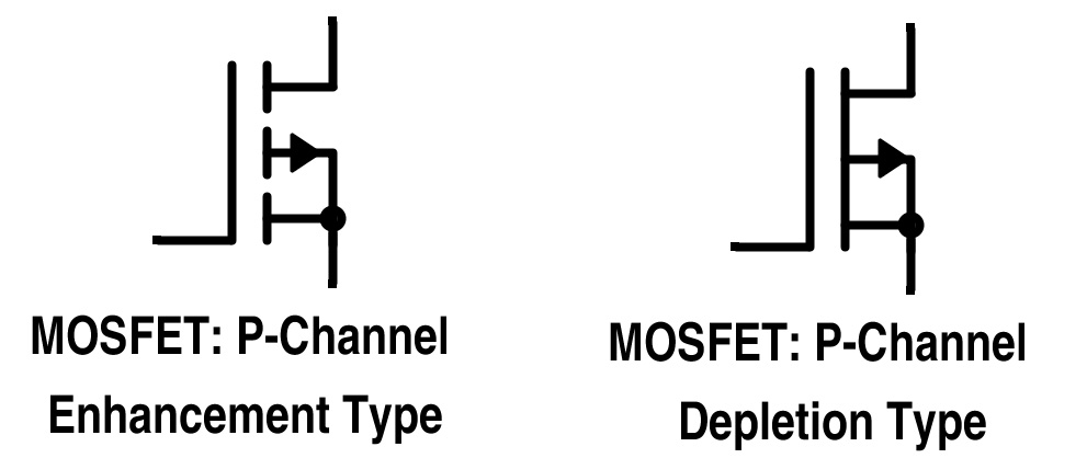
Enhancement(left) and Depletion(right) PMOS Symbol
In a PMOS transistor, when a negative voltage is applied to the gate terminal relative to the source terminal, it creates an electric field that repels holes towards the source and drain terminals. This forms a conductive channel between these two terminals allowing current to flow through.
PMOS Advantages Over NMOS
The main advantage of PMOS transistors is their lower power consumption in 'ON' state compared to NMOS transistors. They also tend to have better noise margin than NMOS circuits which can make them more reliable in certain applications.
PMOS Disadvantages Over NMOS
However, there are downsides with PMOS technology as well: they switch slower than NMOS transistors due to hole mobility being less than electron mobility; this makes them less suitable for high-speed applications. Additionally, because they cannot be made as small as equivalent NMOS devices (due again to hole properties), they don't allow for as dense and compact integrated circuits. Despite these limitations, PMOS was widely used before NMOS technology became prevalent due its simpler manufacturing process.
PMOS refers to an n-type substrate, a p-channel, and a MOS transistor that transports current by the flow of holes.
The hole mobility of the P-channel MOS transistor is low, so when the geometric size of the MOS transistor and the absolute value of the operating voltage are equal, the transconductance of the PMOS transistor is smaller than that of the N-channel MOS transistor. In addition, the absolute value of the threshold voltage of the P-channel MOS transistor is generally high, requiring a relatively high operating voltage. The voltage and polarity of its power supply are incompatible with bipolar transistors—transistor logic circuits. Due to the large logic swing, long charging and discharging process, and the small transconductance of the device, PMOS works at a lower speed. After the emergence of NMOS circuits (see N-channel metal-oxide-semiconductor integrated circuits), most of them have been adopted by NMOS circuits. replace. However, because the PMOS circuit technology is simple and the price is cheap, some medium-scale and small-scale digital control circuits still use PMOS circuit technology.
PMOS vs NMOS: Structure
The structures of NMOS and PMOS transistors are similar in many ways, but there is a key difference in the types of semiconductor materials used.
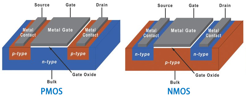
PMOS MOSFET(Left) and NMOS MOSFET(Right) Structure
Here's a basic description:
NMOS Structure
Substrate: The substrate (or body) is made up of p-type semiconductor material.
Source and Drain Regions: Two n-type regions are diffused into the substrate to form the source and drain.
Gate: A thin layer of silicon dioxide (insulator) is grown on top of the substrate between source and drain, over which a conductive gate material (often polysilicon or metal) is deposited.
Operation: When positive voltage applied to gate w.r.t source , it attracts free electrons towards SiO2 layer creating an inversion layer or channel for current flow between source & drain.
PMOS Structure
Substrate: The substrate (or body) consists of n-type semiconductor material.
Source and Drain Regions: Two p-type regions are diffused into the substrate to form the source and drain.
Gate: Similar as NMos, here also silicon dioxide layer separates gate from body with conductive material forming Gate electrode above it.
Operation: When negative voltage applied at Gate terminal w.r.t Source , it repels electrons away from SiO2 interface causing holes accumulation near this surface thus making path for current flow between Source & Drain.
In both cases, controlling voltage on Gate regulates conductivity between Source & Drain . This principle allows MOSFETs to function as amplifiers or switches within circuits.
NMOS vs PMOS: Application
Both NMOS and PMOS transistors are used extensively in digital circuits. They each have their own advantages which make them suitable for different applications.
NMOS Application
Digital Logic Circuits: Due to their high electron mobility, NMOS transistors can switch on and off more rapidly than PMOS, making them ideal for use in high-speed digital logic circuits.
Microprocessors: High speed microprocessors often utilize NMOS technology due to its faster switching times.
Memory Units: Dynamic Random Access Memory (DRAM) cells traditionally used a single transistor (often an NMOS transistor) and a capacitor.
PMOS Application
Low Power Applications: Since they consume less power when 'ON' compared to equivalent nMOSH devices, PMos are often preferred in low-power or battery-operated devices where power consumption is a critical factor.
Pull-Up Resistors: In CMoS logic gates , Pmos transistors are typically used as pull-up resistors due to their ability to maintain strong '1' signal while Nmos provides strong '0'.
Analog Switches & Multiplexers: P-type MOSFETs can be found in analog switches, multiplexers etc because of the need of both type of devices depending upon the application requirement .
NMOS vs PMOS: Which is Better
Electrons (charge carriers in NMOS) have higher mobility than holes (charge carriers in PMOS). This results in faster operation and is useful in high-speed applications. Generally, NMOS fabrication is slightly less expensive. NMOS transistors typically consume more power, particularly in the 'on' state.
PMOS transistors have lower leakage current compared to NMOS when in the 'off' state.PMOS devices are more robust against high-voltage environments. Due to lower hole mobility, PMOS transistors are generally slower than NMOS.
The choice between NMOS and PMOS depends on the specific requirements of the application. For high-speed and low-cost applications, NMOS is often preferred. For applications requiring low leakage current and high-voltage tolerance, PMOS is better suited.

Combined use of NMOS and PMOS
In many modern circuits, both NMOS and PMOS are used together in a complementary fashion (CMOS - Complementary Metal-Oxide-Semiconductor). This approach combines the advantages of both, allowing for efficient and power-saving designs, especially in digital integrated circuits.
Compare NMOS and PMOS
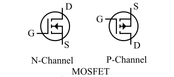
MOS tubes are divided into N-channel and P-channel. We often use NMOS because of its small on-resistance and easy fabrication. It can be seen on the schematic diagram of the MOS tube that there is a parasitic diode between the drain and the source. This is called a body diode. This diode is very important when driving an inductive load (such as a motor). By the way, the body diode only exists in a single MOS tube, and it is usually not inside the integrated circuit chip.
NMOS vs PMOS| Aspect | NMOS (N-type Metal-Oxide-Semiconductor) | PMOS (P-type Metal-Oxide-Semiconductor) |
|---|
| Majority Charge Carriers | Electrons | Holes (Positive Charge Carriers) |
| Semiconductor Type | n-type | p-type |
| Gate Voltage Control | Positive Voltage | Positive Voltage |
| Operation | Conducts when Gate is Positive | Conducts when Gate is Negative |
| Switching Speed | Faster Switching Speed | Slower Switching Speed |
| Power Consumption | Higher Power Consumption | Lower Power Consumption |
| Noise Immunity | Lower Noise Immunity | Higher Noise Immunity |
| Applications | High-Speed Digital Circuits, Microprocessors, Memory Cells, Integrated Circuits | Low-Power Digital Circuits, CMOS Technology, Analog Amplifiers, Voltage Level Shifters, Power Management Circuits |
Conclusion
In conclusion, the differences between NMOS and PMOS transistors highlight the diverse spectrum of semiconductor technology. NMOS, with its higher electron mobility and cost-effectiveness, excels in speed and efficiency, making it ideal for high-speed applications. On the other hand, PMOS, characterized by its lower leakage current and robustness in high-voltage environments, provides reliability and stability, especially in power-sensitive applications.
The harmonious integration of both NMOS and PMOS in CMOS technology epitomizes the innovation in electronics, paving the way for more energy-efficient, high-performance devices. As technology continues to evolve, the complementary roles of NMOS and PMOS transistors are likely to become even more pivotal in shaping the future of electronic circuit design.

Nantian Electronics a professional distributor of electronic components, providing a wide range of electronic products, saving you a lot of time, effort and cost through our meticulous order preparation and fast delivery service.
Share this post


Frequently Asked Questions
1. What does PMOS mean?
PMOS stands for P-type Metal-Oxide-Semiconductor. It's a type of MOSFET (Metal Oxide Semiconductor Field Effect Transistor) where the majority carriers are holes.
2. What does NMOS mean?
NMOS stands for N-type Metal-Oxide-Semiconductor. It's another type of MOSFET, but in this case, the majority carriers are electrons.
3. What is the difference between NMOS and PMOS noise?
The noise characteristics can depend on various factors including process technology and circuit design. However, generally speaking, both types would have similar kinds of intrinsic electronic noise such as thermal noise or flicker (1/f) noise.
4. What is the difference between NMOS and PMOS capacitance?
The gate capacitances of NMos & PMos transistors depend upon their physical dimensions , oxide thickness etc . In a given technology node if both devices are sized similarly they will have comparable gate capacitances.
5. How do I know if my transistor is NMOS or PMOS?
This typically requires knowledge about how the device was fabricated - whether it uses n-type or p-type semiconductor material as its substrate. Another way to tell is by checking its behavior: an nMOSH turns 'on' when a positive voltage applied at Gate while pMOSH needs negative voltage to turn ON.
6. What is the disadvantage of PMOS compared to NMOS?
PMOs has slower switching speed due to lower mobility of holes (charge carriers in Pmos) compared to electrons which are charge carriers in Nmos.
7. Why NMos better than Pmos?
Nmos devices switch faster thanks high electron mobility & also they can be made smaller than equivalent pMos device leading to higher density circuits.
8. Why is NMOS much faster than PMOS?
The speed of a transistor depends on the mobility of the charge carriers that flow through it. In an NMOS transistor, these are electrons, which have higher mobility than holes (the charge carriers in a PMOS transistor). This means that for the same applied voltage, electrons will move faster and thus make NMOS transistors switch faster.
9. What are two differences between NMOS and PMOS?
Substrate Material: The substrate material for an NMOS is p-type semiconductor while for a PMOS it's n-type.
Charge Carriers: In an NMOS, majority charge carriers are electrons whereas in a PMos they're holes.
10. What are the advantages of PMOS?
PMOS transistors offer several benefits that make them advantageous for various applications. They consume less power in the 'ON' state compared to NMOS devices, which is particularly beneficial for low-power and battery-operated applications. In CMOS logic gates, they provide a strong '1' logic level, enhancing the overall performance of digital circuits.
PMOS circuits also have better noise margins than NMOS circuits, increasing their reliability in noisy environments. The manufacturing process of PMOS is simpler and more cost-effective than that of complementary MOS (CMoS) or NMos processes. Additionally, due to their high resistance when turned off, PMOS transistors are commonly used as pull-up resistors in CMoS technology.
11. Is Pmos bigger than Nmos?
Yes, typically because hole mobility is less than electron mobility resulting larger device sizes to achieve same current drive capability.
12. Why is Cmos better than Nmos and PmoS?
CMoSH combines best features both technologies i.e., fast switching from nMosh & low static power consumption from pMosH . This makes circuits more energy efficient , particularly important battery powered or portable devices.
13. Why is PMOS slower?
PMOS transistors are slower than NMOS transistors primarily because of the difference in charge carrier mobility. In PMOS, the majority carriers are holes, while in NMOS, they are electrons.
Electrons have a higher mobility than holes due to their smaller effective mass and different interaction with the semiconductor lattice. This means that for a given electric field strength, electrons can move faster through the transistor than holes can.
As a result, when an electric signal is applied to a PMOS transistor (which relies on hole movement), it will switch states more slowly compared to an NMOS transistor (which relies on electron movement). Hence we say that "PMos is slower".