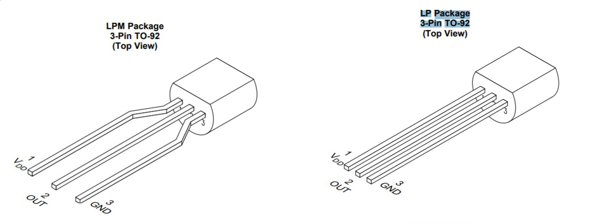
The T0-92 package(TO92 or T092 Package), which stands for "Transistor Outline Package, Case Style 92," is a type of single-piece, through-hole casing for semiconductors commonly used for low-power components such as NPN and PNP bipolar junction transistors, field-effect transistors, and other logic or amplifying devices. Composed of lightweight, cost-effective plastic and having three leads (representing the parts of a transistor or transistor-like component), this package is noted for its simplicity and widespread usage.
What is T092 Transistor
A T092 transistor is a type of semiconductor device packaged in the T0-92 case style. The T092 package is a small, cylindrical package with three leads arranged in a triangular pattern. It is commonly used for transistors, particularly bipolar junction transistors (BJTs) and small-signal field-effect transistors (FETs).
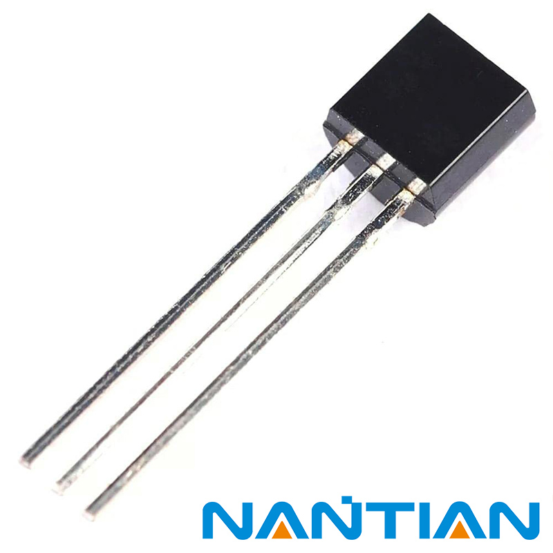
Key characteristics of a T092 transistor:
1. Package: The transistor is encased in a cylindrical plastic or epoxy package with a diameter of about 4.5 mm and a height of about 4.5 mm.
2. Leads: The package has three leads that are arranged in a triangular pattern, with a lead spacing of 1.27 mm (0.05 inches). The leads are typically labeled as collector (C), base (B), and emitter (E) for BJTs, or as drain (D), gate (G), and source (S) for FETs.
T092 transistors have a relatively low power dissipation capability, typically around 0.5 to 1 watt, depending on the specific device and operating conditions.TO-92 transistors are commonly used in low-power electronic circuits, such as amplifiers, switches, voltage regulators, and logic gates.
Examples of popular T092 transistors include:
To-92 package dimensions
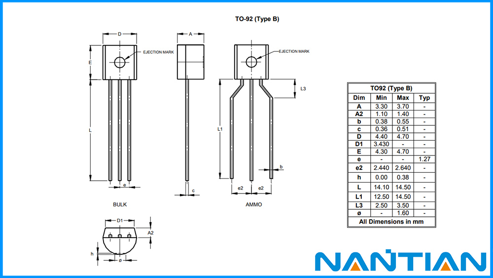
To92 Transistor Dimension
The T092 package, a type of plastic molding encapsulation used in semiconductor devices like transistors, usually adheres to the following typical dimensions:
1. Body length: 4.5 mm
2. Body width: 3.5 mm
3. Body height: 4.5 mm
4. Pin pitch (distance between the centers of adjacent pins): 1.27 mm
5. Pin length (varies depending on whether it's the short or long form): 13 mm for the short form and 19 mm for the long form, straight from the molding body.
T0 92 Advantage
The TO-92 package has several key advantages that have made it a popular choice for low-power transistors and other semiconductor devices:
1. Cost-efficiency: TO-92 packages are made from a low-cost, lightweight plastic, which makes them economical for mass production.
2. Ease of debugging: The through-hole technology used in these packages allows for easy insertion and removal from a board, which is advantageous during prototyping and debugging stages of development.
3. Ease of soldering: As through-hole packages, TO-92 devices can often be soldered more easily and securely than surface mount devices.
4. Durability: The larger size and through-hole design makes TO-92-packaged components physically stronger and less prone to being damaged by handling, compared to smaller, surface-mounted components.
5. Heat dissipation: While still limited compared to larger packages, TO-92 devices can typically dissipate more heat than equivalent surface-mount devices.
6. Compatibility: The TO-92 package is widely recognized and used across numerous applications, making it compatible with a wide range of circuits and designs.
The TO-92 package is more suitable for low-power applications. As power requirements increase, components may need to be housed in larger packages that can dissipate heat more effectively.
TO 92 Disadvantage
While the TO-92 package has many advantages, it also has some notable disadvantages:
1. Limited power dissipation: The TO-92 package is typically used for low-power applications due to its small size and plastic construction, which are not capable of dissipating large amounts of heat. For high-power applications, you'd need larger, metal packages that are better at heat dissipation.
2. Larger size: Compared to surface-mount devices (SMD), through-hole devices like those in the TO-92 package are significantly larger. This could become a problem for densely populated or miniaturized circuits.
3. More time-consuming assembly: Assembly of through-hole devices typically takes more time (and hence can cost more) compared to surface-mounted devices, especially for automated assembly processes.
4. Single-sided board use: Once a TO-92 device is soldered to a circuit board, the side of the board it's soldered to becomes practically unusable for placing other components or for routing tracks.
5. Not suitable for high-speed circuits: The longer leads and higher lead inductance of through-hole packages can introduce problems in high-frequency or high-speed circuits.
The TO-92 package is more suitable for low-power applications. As power requirements increase, components may need to be housed in larger packages that can dissipate heat more effectively. Those working on electronics designs should weigh the trade-offs of using TO-92 packages versus other packages based on the specific requirements of the circuit and the environment in which it will be used.
T092 Package Application Scenarios
The TO-92 package is a compact, cylindrical package commonly used for small electronic components such as transistors, diodes, and voltage regulators. It has three leads arranged in a triangular pattern, with the package material providing electrical insulation and protection. TO-92 packages are known for their small size, low power dissipation capability, and widespread use in various electronic applications.
Common components available in TO-92 packages include bipolar junction transistors (BJTs), field-effect transistors (FETs), small-signal diodes, voltage regulators, temperature sensors, operational amplifiers, Hall effect sensors, optocouplers, and audio amplifiers. These components find applications in diverse areas such as small-signal amplification, switching and logic circuits, power supply regulation, temperature sensing and control, signal conditioning, motor control, isolation and protection, sensor interfacing, automotive electronics, and hobby and DIY projects. The compact size and low power requirements of TO-92 packaged components make them suitable for space-constrained and battery-powered applications.
Common components in a TO-92 Package
Common electronic components that are available in TO-92 packages include:
1. Bipolar Junction Transistors (BJTs)
NPN transistors (e.g., 2N2222, 2N3904, BC547)
PNP transistors (e.g., 2N2907, 2N3906, BC557)
2. Field-Effect Transistors (FETs)
Junction FETs (JFETs) (e.g., 2N5457, 2N5460)
MOSFETs (e.g., 2N7000, BS170)
3. Small-Signal Diodes
4. Voltage Regulators
Fixed linear voltage regulators (e.g., 78L05, 79L05)
Adjustable linear voltage regulators (e.g., LM317L, LM337L)
5. Temperature Sensors
6. Operational Amplifiers
7. Hall Effect Sensors
8. Optocouplers
9. Audio Amplifiers
These are just a few examples of the many electronic components available in TO-92 packages. The specific choice of component depends on the application requirements, such as voltage and current ratings, frequency response, and noise characteristics.
TO-92 and TO-92S packages
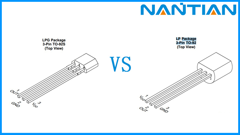
T092S Transistor vs T092 Transistor
The TO-92 and TO-92S packages are both widely used for small electronic components, but they have some differences in their design and dimensions. Here's a comparison of the two packages:
| TO-92 package | TO-92S package |
|---|
| Lead arrangement | The three leads are arranged in a triangular pattern, with the leads emerging from the same side of the package. | The three leads are arranged in a inline pattern, with the leads emerging from the same side of the package. |
| Lead spacing | The lead spacing is typically 1.27 mm (0.05 inches) between the leads. | The lead spacing is typically 2.54 mm (0.1 inches) between the leads, which is larger than the TO-92 package. |
| Package dimensions | The standard TO-92 package has a diameter of about 4.5 mm and a height of about 4.5 mm. | The TO-92S package has similar dimensions to the TO-92 package, with a diameter of about 4.5 mm and a height of about 4.5 mm. |
| Package shape | The package has a cylindrical shape with a flat side, often indicating the emitter lead for BJTs. | The package has a cylindrical shape with a flat side, similar to the TO-92 package. |
| Popularity | The TO-92 package is more common and widely used compared to the TO-92S package. | The TO-92S package is less common compared to the standard TO-92 package. |
The main difference between the two packages lies in the lead arrangement and spacing. The TO-92 package has a triangular lead arrangement with a smaller lead spacing, while the TO-92S package has an inline lead arrangement with a larger lead spacing.
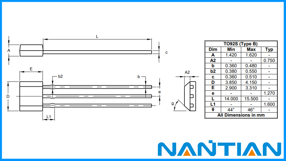
TO92S Package Outline Dimensions
The choice between T0-92 and T0-92S packages depends on factors such as the specific component, PCB layout requirements, and manufacturing processes. The T0-92 package is more widely used and compatible with a larger range of components, while the T0-92S package may be preferred in certain situations where the inline lead arrangement or larger lead spacing is beneficial.
T0 92 Transister Package FAQ
1. What is TO-92 in transistors?
TO-92 is a common package type for small transistors and other semiconductor devices. It has a compact, cylindrical shape with three leads arranged in a triangular pattern. The package is made of plastic or epoxy and provides electrical insulation and protection for the internal transistor die. TO-92 packages are widely used for small-signal bipolar junction transistors (BJTs) and field-effect transistors (FETs) in various electronic applications.
2. What is the thermal resistance of TO-92?
The thermal resistance of a TO-92 package depends on the specific device and the mounting conditions. Typically, the thermal resistance from junction to ambient (θJA) for a TO-92 package ranges from 150°C/W to 200°C/W. This means that for every watt of power dissipated by the transistor, the junction temperature will rise by 150°C to 200°C above the ambient temperature.
3. What is size of T092 Transister?
The TO-92 transistor package is a small, cylindrical package with a typical body diameter and height of 4.5 mm, lead spacing of 1.27 mm, and overall length of 8.5 mm to 10 mm.