1. Introduction
Modern precision electronic devices face a universal and fatal threat: ElectroStatic Discharge (ESD). The static electricity generated in our daily lives, such as when plugging or unplugging cables in a dry environment, can instantly release high voltages measuring thousands of volts (kV).

As chip manufacturing processes continue to advance, integrated circuits are becoming less tolerant of high voltage. An ESD pulse of several kilovolts, lasting only nanoseconds, is enough to instantly burn out the input terminals of sensitive chips, causing irreversible physical damage. Static electricity is the number one invisible killer of electronic product reliability.
So, how do engineers build a robust line of defense for sensitive chips within thin, compact devices?
Today, we introduce our main subject: the PESD5V0U1BL,315 from Nexperia. It is neither a processor nor memory, but it is an indispensable "ESD safeguard" found in almost all modern electronic devices. This minuscule component is a key cornerstone ensuring the stable and reliable operation of our cell phones, computers, automotive electronics, and more. In the following sections, we will fully analyze this tiny, yet powerful electronic guardian.
2. PESD5V0U1BL,315 Core Technology Deep Dive
Before diving into the operational principles of the PESD5V0U1BL, let's review its technical "ID card." These parameters are precisely what make it irreplaceable in high-speed, high-reliability designs.
Key Product Specifications (Based on Representative PESD5V0U1BL Series Data)
| Parameter | Symbol | Typical Value / Standard | Technical Significance |
|---|
| Manufacturer | Nexperia | Nexperia | A global leader in discrete devices |
| Type | | Single-line Bidirectional ESD Protection Diode | Protects a single data line from both positive and negative static shocks |
| Ultra-Low Capacitance | Cd | Typical 0.95pF | Ensures high-speed signal integrity |
| Clamping Voltage | V CL | Typical 8V | The maximum voltage the protected chip end is exposed to during an ESD event |
| Reverse Standoff Voltage | V RWM | 5.5V Max | Suitable for 5V and 3.3V interfaces |
| ESD Immunity | | IEC 61000-4-2, Level 4 | Withstands 8kV contact discharge |
| Leakage Current | I RM | Typical 1 nA | Ultra-low power consumption, ideal for battery-powered devices |
| Package | | DFN1006-2 (or SOD-882) | One of the smallest packages in the industry (1.0 x 0.6 mm) |
Core Technology Interpretation: Exceeding Traditional Protection Performance
1. Ultra-Low Capacitance: The Cornerstone of Signal Integrity
This model's core strength lies in its ultra-low diode capacitance. The datasheet clearly indicates that its typical capacitance value can be as low as 0.95 picofarads (pF). Why is capacitance so critical?
For high-speed data transmission, such as USB 2.0, Ethernet, or even higher-spec HDMI interfaces, any added capacitance on the data line causes signal delay and attenuation, negatively impacting Signal Integrity. High capacitance acts like a "brake" on the data channel, leading to signal waveform distortion, eye diagram degradation, and ultimately, data transmission errors or connection failures.
This figure of 0.95 pF makes it the ideal choice for protecting high-speed interfaces operating at megabits (Mbps) and even gigabits (Gbps), making stable high-speed data transfer possible.
2. Excellent Clamping Voltage: Activating the ESD "Safety Lock"
When an ESD event occurs, the response speed and clamping capability of the protection device are paramount.
Definition: Clamping Voltage (V CL) is the highest voltage level the ESD protection device suppresses the transient to after it quickly turns on. This is the voltage the downstream sensitive chip must actually withstand.
Performance: The PESD5V0U1BL features an ultra-low clamping voltage (typical 8 volts). This means that even when faced with a static shock of several kilovolts, it reacts within nanoseconds, limiting the voltage to a safe region around 8 volts. This maximally protects the delicate chip from high-voltage damage.
3. The Perfect Blend of High Reliability and Low Power Consumption
Robust ESD Immunity: This model fully meets the highest international standard, IEC 61000-4-2 Level 4, capable of withstanding up to 8 kilovolts of contact discharge. This ensures the product passes stringent Electromagnetic Compatibility (EMC) testing.
Ultra-Low Leakage Current: Under normal operating voltage, its leakage current (I RM) is extremely low, typically just 1 nanoampere (nA). This characteristic is crucial for any battery-powered portable device (such as cell phones or wearables), ensuring the protection device does not become an unnecessary power drain while the device is in standby mode.
3. Product Features and Package Advantages
Beyond its core electrical protection performance, the widespread adoption of the PESD5V0U1BL series protection devices globally is also due to its sophisticated package design and high-standard quality certifications. These features collectively ensure the device's reliability and ease of use in practical applications.
1. Unidirectional Protection Design: Precise Defense for Specific Lines
Within the PESD5V0U1BL family, there are models featuring a Unidirectional protection design. This design is primarily used to protect single-polarity signal lines, such as power supply lines or control signal lines that have a fixed positive voltage.
The advantage of the unidirectional design lies in its focus, allowing it to provide optimized clamping and response performance specifically against shocks of a particular polarity. In an engineer's design, when it is clearly known that the static shock will only endanger the circuit from one direction, choosing unidirectional protection offers a more precise and stable protective effect.
2. Ultra-Small Package: The "Micro-Art" of Boosting Production Efficiency
The PESD5V0U1BL and its sister products utilize ultra-small surface-mount device (SMD) plastic packages, such as the SOD882D, which are leadless.
Extremely Small: These packages measure only 1.0 millimeter by 0.6 millimeter, making them key to achieving the thin and light design of modern smart devices (like wearables and TWS earbuds). On space-constrained circuit boards, this size advantage allows design engineers to place more functional components.
Design Convenience: Notably, many leadless packages are designed with visible and solderable side pads. This detail is highly significant on an automated production line. It allows optical inspection equipment to more easily confirm the connection status of the pads, reducing the risk of soldering defects. Consequently, this contributes to a higher yield rate in mass production, indirectly lowering product manufacturing costs.
3. Automotive-Grade Certification: Guarantee of High Reliability
Many models in this series have obtained AEC-Q101 Automotive-Grade Certification. This is not just a quality label; it represents that the device must meet the automotive industry's most stringent standards during design, manufacturing, and testing.
Harsh Environment Suitability: Automotive electronics must operate reliably long-term in environments with extreme temperature variations, humidity, and mechanical vibration. Achieving AEC-Q101 certification proves that this protection device possesses the ability to maintain high performance and high reliability under these severe conditions.
Quality Endorsement: For engineers in the industrial and automotive application fields, choosing a device with this certification means selecting the highest level of quality assurance, which is crucial for safety-critical automotive systems.
4. Application Scenarios
The PESD5V0U1BL family is widely adopted across numerous industries due to its excellent protection and low capacitance characteristics:
Computers and peripherals
Audio and video equipment
Cellular handsets and accessories
10/100/1000 Mbit/s Ethernet
Communication systems
Portable electronics
SIM card protection
USB, High-Definition Multimedia Interface (HDMI), FireWire
High-speed data lines
5. Package Outline

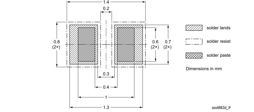
6. PESD5V0U1BL,315 Soldering
Why Choose the PESD5V0U1BL,315?
Ultra Low Load Capacitance: The typical capacitance value is only 0.95 picofarads (pF). This specification ensures that when protecting high frequency differential signals such as USB 3.0, HDMI 2.0, DisplayPort, or Gigabit Ethernet, the signal eye diagram remains open, avoiding Signal Integrity issues.
Low Clamping Voltage: During an electrostatic discharge event, the device quickly clamps the voltage to a low level, typically around 8 volts (V). This provides a substantial safety margin for precise controller chips operating at 3.3 volt and 5 volt levels.
Transient Response Speed: It features a response time in the nanosecond (ns) range, allowing it to turn on rapidly before the static pulse reaches the sensitive chip, effectively diverting the energy to the ground.
Ultra Miniature Size: Utilizing the DFN1006-2 package, the external dimensions are only 1.0 millimeter by 0.6 millimeter, making it one of the smallest protection devices in the industry.
Saves Board Space: The minuscule footprint allows engineers to easily integrate protection functionality into space constrained products, such as smartwatches, wireless earbuds, or micro sensor modules.
Get Instant Online Quote
Frequently Asked Questions (FAQ) about PESD5V0U1BL,315
1. What is the primary function of this device?
It protects a single data line from damage caused by Electrostatic Discharge (ESD) and other voltage transients.
2. Is it a unidirectional or bidirectional protector?
It is a bidirectional ESD diode, meaning it handles both positive and negative static events.
3. What is its major technical advantage?
Ultra low capacitance (typically 0.95 picofarads) to ensure signal quality on high speed lines without signal degradation.
4. What is the physical size of the component?
It uses the ultra small DFN1006-2 package, measuring just 1.0 millimeter by 0.6 millimeter.
5. What is its standard operating voltage?
The reverse standoff voltage is 5.0 Volts, making it suitable for both 5V and 3.3V interfaces.
6. What is its ESD immunity rating?
It meets the highest industry standard, IEC 61000-4-2 Level 4, withstanding 8 kilovolts contact discharge.
7. What type of interfaces does it protect?
High speed data lines including USB, HDMI, Gigabit Ethernet (10 100 1000 Mbit per second), and SIM card protection.


