Among the various types of transistors, the NMOS (N-Channel Metal-Oxide-Semiconductor) transistor has gained significant popularity due to its unique characteristics and wide range of applications. In this comprehensive guide, we will dive deep into the world of NMOS transistors, exploring their structure, symbol, working principles, current equation and functional characteristics.
What is NMOS?
NMOS stands for N-Channel Metal Oxide Semiconductor. It means N-type metal-oxide-semiconductor, and transistors with this structure are called NMOS transistors. MOS transistors are divided into P-type MOS transistors and N-type MOS transistors. An integrated circuit composed of MOS tubes is called a MOS integrated circuit. A circuit composed of NMOS is an NMOS integrated circuit. A circuit composed of PMOS tubes is a PMOS integrated circuit. A complementary MOS circuit composed of NMOS and PMOS tubes is a CMOS circuit.
Introduction to NMOS transistors
NMOS transistors, standing for N-type Metal-Oxide-Semiconductor transistors, are fundamental components in the realm of semiconductor technology, powering a myriad of electronic devices from the simplest circuits to the most complex microprocessors. At their core, NMOS transistors leverage the electrical properties of n-type semiconductor materials, which are silicon substrates doped with elements that provide an abundance of free electrons, to act as efficient switches or amplifiers within electronic circuits.
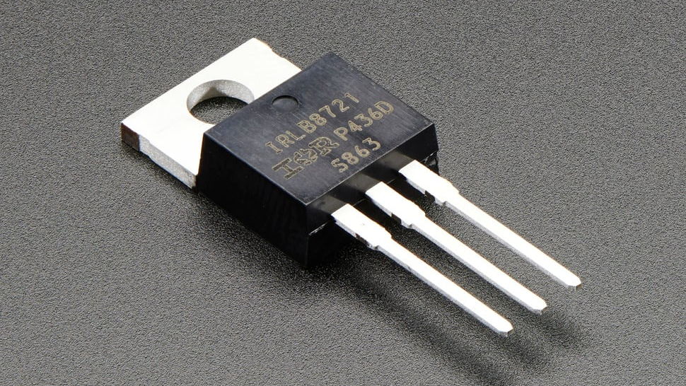
Nmos transistor IRLB8721
NMOS transistors are usually divided into two types:
NMOS transistors Symbol
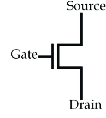
NMOS Transistor Symbol(N-Channel MOSFET Symbol)
The symbol for n channel mosfet represents the device's basic functionality and structure in a simplified form. It includes three terminals: the Gate (G) controlling the flow of current, the Drain (D) where current exits, and the Source (S) where current enters. The outward-pointing arrow on the Source indicates the flow direction of n-type carriers (electrons). A broken line between the Drain and Source represents the n-type channel, which forms when sufficient voltage is applied to the Gate, allowing current to flow. The Gate line not touching the channel symbolizes the insulating oxide layer between the Gate and the substrate/channel in the actual NMOS structure, illustrating the transistor's operation principle: controlling the conductive channel between Source and Drain through Gate voltage to manage current flow.
For a more intuitive understanding, the picture below is the pin arrangement of the IRF540N MOSFET.
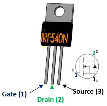
IRF540N MOSFET pin arrangement from left to right: Gate, Drain, Source
N-Channel Depletion-Mode MOSFETs Symbol
The N-channel Depletion-Mode MOSFETs Symbol are called NMOS Depletion-Mode Symbol and they are represented by the following symbols:
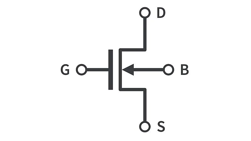
N-Channel Depletion-Mode Symbol
Components of the symbol:
G: Gate terminal
D: Drain terminal
S: Source terminal
The line with the arrow between source and drain represents the channel, and the arrow points from source to drain, indicating the direction of conventional current flow when the device is on.
The broken line in the channel (|<) indicates that it's a depletion-mode device.
Characteristics of NMOS depletion-mode devices:
They are normally on at VGS = 0V due to the presence of a conducting channel.
To turn off the device, a negative gate-to-source voltage (VGS < 0) must be applied to deplete the channel of charge carriers.
As the negative VGS increases in magnitude, the depletion region widens, and the channel conductivity decreases until the device is fully turned off (pinch-off).
They are less commonly used compared to enhancement-mode devices, which are normally off at VGS = 0V.
Depletion-mode MOSFETs are used in certain analog circuits, such as in current sources, active loads, and in some logic circuits. However, enhancement-mode devices are more widely used in digital and switching applications.
N-Channel Enhancement-Mode MOSFETs Symbol
The picture below shows p channel enhancement-mode mosfet symbol.
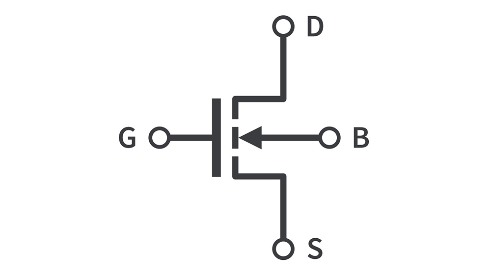
NMOS Enhancement Mode Symbol
Here's the symbol and its meaning:
Components of the symbol:
G: Gate terminal
D: Drain terminal
S: Source terminal
The line with the arrow between source and drain represents the channel, and the arrow points from source to drain, indicating the direction of conventional current flow when the device is on.
The solid line in the channel (|) indicates that it's an enhancement-mode device.
Characteristics of NMOS enhancement-mode devices:
They are normally off at VGS = 0V because there is no conducting channel initially.
To turn on the device, a positive gate-to-source voltage (VGS > VTH) must be applied to attract electrons and create an inversion layer, forming a conductive channel between the source and drain.
The threshold voltage (VTH) is the minimum VGS required to create the channel and turn on the device.
As VGS increases above VTH, the channel conductivity increases, allowing more current to flow from drain to source.
Enhancement-mode devices are more commonly used than depletion-mode devices, particularly in digital circuits and as switches.
NMOS enhancement-mode devices are widely used in various applications, such as:
The enhancement-mode operation provides better control over the device's switching characteristics and allows for the creation of more efficient and compact circuits compared to depletion-mode devices.
Nmos Transistor Structure
The structure of an NMOS (N-type Metal-Oxide-Semiconductor) transistor is made up of several key components:
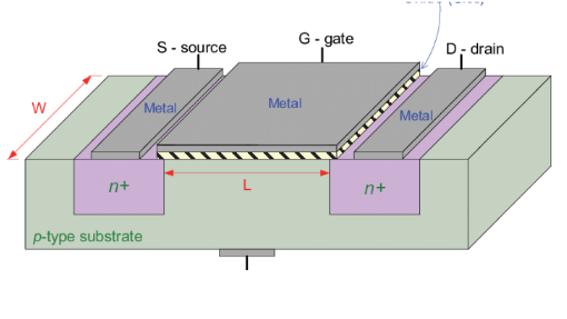
nmos transistor structure diagram
Substrate: The base layer of the NMOS transistor is called the substrate, typically made of p-type silicon. This is the bulk material that forms the body of the device.
Source and Drain: On top of the substrate, there are two regions heavily doped with n-type impurities, known as the source and the drain. These regions are where electrons enter and exit the transistor.
Gate: The gate is the control terminal of the transistor. It is situated above the substrate but is separated from it by a very thin insulating layer. The gate is usually made of polysilicon or metal.
Oxide Layer: Between the gate and the substrate is a thin layer of silicon dioxide (SiO₂) or another insulating material. This layer is crucial as it insulates the gate from the substrate, allowing the gate to control the flow of electrons between the source and drain without direct contact.
N-type Channel: When a positive voltage is applied to the gate, it attracts electrons from the substrate to form an n-type channel between the source and drain under the gate area. This channel is the path through which current flows in the transistor.
Contacts and Interconnections: Metallic contacts are made to the source, gate, and drain to allow for electrical connection to the rest of the circuit.
The structure of an NMOS transistor is ingeniously simple yet effective, consisting of three main terminals: the source, drain, and gate. The source and drain are made of n-type material, while the gate is separated from the underlying silicon substrate by a thin insulating layer of silicon dioxide. This design allows the gate voltage to control the flow of electrons between the source and drain, enabling or disabling the conduction path based on the applied electrical signals. The brilliance of NMOS technology lies in its ability to perform rapid switching with low power consumption, making it a cornerstone of digital electronics that has shaped the modern electronic landscape.
NMOS transistor working principle
An NMOS transistor consists of a source, a drain and a control electrode. When the voltage on the control terminal is higher than the source terminal, the transistor turns on, allowing current to flow from source to drain. When the voltage on the control electrode is lower than the source, the transistor turns off, preventing current from flowing from source to drain.
Functional characteristics of NMOS transistors
An NMOS transistor acts as a closed circuit when it receives a non-zero voltage, meaning the connection between source and drain acts as a wire. Therefore, the power supply receives current from the gate terminal. When this transistor gets a voltage of about 0V, the connection between the source terminal and the drain is broken, creating an open circuit, causing current to flow from the gate terminal to the drain.
The I-V properties of NMOS transistors are shown below. The voltage between source and drain (VDS) and between gate and source (VGS). Therefore, the curve between IDS and VDS is obtained by simply connecting the terminals of the power supply to ground, setting the initial VGS value, and then stepping the VGS value from "0" to "VDD" to set VDS to the highest DC voltage value . Therefore, IDS is very small and will show a linear trend for very low VGS. When the VGS value rises, IDS improves and develops the following dependencies on VGS and VDS.
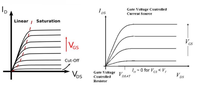
NMOS transistor characteristic curves and working modes
Case of VGS=0
There are two back-to-back PN junctions between the drain d and source s of the enhancement mode MOS tube. When the gate-source voltage VGS=0, even if the drain-source voltage VDS is added, and regardless of the polarity of VDS, there is always a PN junction in a reverse biased state, and there is no conductive channel between the drain-source. So the drain current iD≈0 at this time.
Case of VGS>0
If VGS>0, an electric field will be generated in the SiO2 insulating layer between the gate and the substrate. The direction of the electric field is perpendicular to the electric field directed from the gate to the substrate on the semiconductor surface. This electric field repels holes and attracts electrons.
Repelling holes: The holes in the P-type substrate near the gate are repelled, leaving immovable acceptor ions (negative ions) to form a depletion layer. Attract electrons: The electrons (minority carriers) in the P-type substrate are attracted to the substrate surface.
Formation of conductive channels
When the VGS value is small and the ability to attract electrons is not strong, there is still no conductive channel between the drain and the source. When VGS increases, more electrons are attracted to the surface layer of the P substrate. When VGS reaches a certain value, these electrons form an N-type thin layer on the surface of the P substrate near the gate and are connected to the two N+ regions. Through, an N-type conductive channel is formed between the drain and the source. Its conductive type is opposite to that of the P substrate, so it is also called an inversion layer. The larger VGS is, the stronger the electric field acting on the semiconductor surface is, the more electrons are attracted to the surface of the P substrate, the thicker the conductive channel is, and the smaller the channel resistance is.
The gate-source voltage when the channel begins to form is called the turn-on voltage, represented by VT.
When VGS<VT, the N-channel MOS tube cannot form a conductive channel and the tube is in a cut-off state. Only when VGS≥VT can a channel be formed. This kind of MOS tube that can form a conductive channel when VGS≥VT is called an enhancement MOS tube. After the channel is formed, a forward voltage VDS is applied between the drain and the source, and a drain current is generated.
Nmos Transistor Current Equation
The current equation for an NMOS transistor operating in the active or saturation region reflects how the device conducts when the gate-source voltage (VGS) exceeds the threshold voltage (Vth), allowing a conductive channel to form between the drain and source. The equation is:
Where:
ID is the drain-source current,
μn is the electron mobility,
Cox is the gate oxide capacitance per unit area,
W is the width of the transistor,
L is the length of the transistor,
VGS is the gate-source voltage, and
Vth is the threshold voltage.
This equation assumes the transistor is in the saturation region, where the drain-source voltage (VDS) is large enough to pinch off the conductive channel at the drain end, creating a constant current flow that's independent of VDS but directly related to VGS. In the linear or triode region, where VDS is smaller and the channel is not pinched off, the current equation is more complex and dependent on both VGS and VDS.
NMOS transistor circuit
Below is a schematic diagram of NOT gate made from NMOS and PMOS transistors. By connecting the pMOS transistor to source and the nMOS transistor to ground, we can combine pMOS and nMOS transistors together to create a NOT gate. Therefore, the circuit will be our first example of a CMOS transistor. One type of logic gate that produces an inverted input as an output is the NOT gate. Inverter is another name for this door. If the input is "0", the result will be "1".
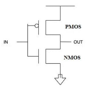
NMOS transistor circuit
The top pMOS transistor and the bottom nMOS transistor receive input when the input is zero. The input value "0" is converted to "1" after reaching the pMOS transistor. Therefore, the source link is severed. So if the connection to the drain (GND) is also closed, this will produce a logic "1" value. We know that an nMOS transistor does not flip the input value; therefore, it accepts the zero as-is and creates an open drain. As a result, the gate generates a logic value of 1.
If the input value is also "1", then the two transistors of the above circuit receive the value "1". The "1" value will become "o" after being received by the pMOS transistor. Therefore, the path to the source is free. The nMOS transistor does not invert after receiving the value "1". Therefore, the input value remains at 1. Once the nMOS transistor receives a value, the connection to GND is closed. Therefore, it will produce an output of logic "0".
Frequently Asked Questions
1. When does an NMOS transistor turn on?
An NMOS transistor turns on when the gate-to-source voltage (VGS) exceeds the threshold voltage (VTH). For enhancement-mode NMOS, VGS must be greater than VTH (typically 0.5V to 1V) to create a conductive channel between the drain and source, allowing current to flow.
2. When does an NMOS transistor turn off?
An NMOS transistor turns off when the gate-to-source voltage (VGS) is below the threshold voltage (VTH). For enhancement-mode NMOS, when VGS is less than VTH, the conductive channel disappears, and the transistor becomes non-conductive, preventing current flow between the drain and source.
3. What does NMOS stand for?
NMOS stands for "N-channel Metal-Oxide-Semiconductor." It refers to a type of field-effect transistor (FET) where the charge carriers are electrons (negative charge carriers) in an N-type conductive channel.
4. Why is NMOS better than PMOS?
NMOS transistors have several advantages over PMOS transistors:
Higher electron mobility: Electrons have higher mobility than holes, allowing NMOS transistors to switch faster and have better performance.
Lower on-resistance: NMOS transistors have lower on-resistance than PMOS transistors of the same size, resulting in less power dissipation.
Smaller size: For the same current drive capability, NMOS transistors can be made smaller than PMOS transistors, enabling higher packing density and more compact circuits.
However, PMOS transistors have their own advantages, such as better noise immunity and suitability for certain analog circuits.
More Information: What is the Difference Between NMOS and PMOS
5. Why is NMOS on for High Voltage?
NMOS transistors are not always on for high voltage. In fact, they are designed to turn off when the gate-to-source voltage (VGS) is below the threshold voltage (VTH). However, there are special types of NMOS transistors called "High-Voltage NMOS" (HV-NMOS) that are designed to handle higher voltages than standard NMOS transistors. These HV-NMOS transistors have a thicker gate oxide and a longer channel length to increase their breakdown voltage, allowing them to operate at higher voltages without damage. They are used in power management circuits, display drivers, and automotive applications where high voltages are present.