Discover unparalleled performance and reliability with the Texas Instruments SN74LVC244AQPWRQ1, an octal buffer and line driver designed specifically for 3.3-V VCC operation but with the capability to provide 5-V tolerant inputs.

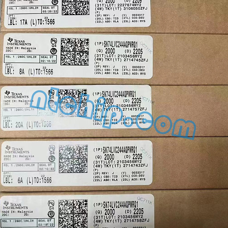
Box Packaging and SN74LVC244AQPWRQ1 Labeling
The SN74LVC244AQPWRQ1 is part of TI’s robust LVC family of components – optimized for low-voltage applications while maintaining high-speed data transfer rates. With eight non-inverting buffers and line drivers in one compact package, this component offers superior design flexibility.
Key Features:
Versatile Performance:This chip operates from a wide supply voltage range (from 2V to 3.6V), ensuring compatibility across various system configurations.
Input Tolerance:The device provides I/Os that are 5-V tolerant allowing it to interface with mixed-voltage systems without any additional external components.
High-Speed Data Transfer: With propagation delay times as low as 4.7 ns, your data moves swiftly where it needs to go.
Robust Design: Manufactured under automotive-grade standards (qualified according to AEC-Q100), this chip ensures reliable operation even in harsh conditions.
Power-Off Protection: The inputs can be active even when VCC is at zero volts which aids in preventing erroneous results due to misreading input lines.
Applications:
The versatile nature of the SN74LVC244AQPWRQ1 makes it ideal for various applications such as:
Data routing
Memory address drivers
Bus transceivers
It also plays a crucial role in automotive systems due to its robust construction under AEC-Q100 standards.
Advantages:
Wide Supply Voltage Range: This chip operates from a wide supply voltage range (from 2V to 3.6V), ensuring compatibility across various system configurations.
Input Tolerance: The device provides I/Os that are 5-V tolerant allowing it to interface with mixed-voltage systems without any additional external components.
High-Speed Data Transfer: With propagation delay times as low as 4.7 ns, your data moves swiftly where it needs to go.
Robust Design: Manufactured under automotive-grade standards (qualified according to AEC-Q100), this chip ensures reliable operation even in harsh conditions.
Power-Off Protection: The inputs can be active even when VCC is at zero volts which aids in preventing erroneous results due to misreading input lines.
Product Parameters:
Function : Buffer/Line Driver
Logic Family : LVC
Number of Bits per Element : 8
Maximum Operating Temperature : +125 °C
Minimum Operating Temperature : -40 °C
Propagation Delay Time: Max tpd @ Nominal Vcc =9 ns