There are many types of parameters of the power IGBT module, and the measurement methods corresponding to different parameters are also quite different. The power IGBT module parameter measurement system measures the key parameters of the measured power IGBT module: saturation voltage, threshold voltage, diode forward voltage, leakage current, breakdown voltage, and collector current. This chapter will introduce in detail the detailed measurement scheme of the power IGBT module parameter measurement system for the parameters measured by the power IGBT module and explain the measurement significance of each parameter
IGBT Saturation Voltage Testing
The saturation voltage is VCE (sat), where sat means saturation (Saturation), and it will also be called VCE (on) in some brands of IGBT manuals. It is often used as a switch in various applications, but it is not an ideal switch itself, and losses will occur during work. IGBT losses are divided into two parts: their own internal losses and anti-parallel diode losses. The internal loss is specifically manifested in: the saturation voltage exists when the IGBT is turned on, and the switching loss occurs when the switch is switched. The saturation voltage is similar to the on-resistance (Rds(on)) of the MOSFET, which directly reflects the self-energy loss of the IGBT when it is turned on. The smaller the VCE(sat), the smaller the loss and the lower the possibility of device overheating. IGBT saturation voltage VCE (sat) is related to gate-emitter voltage VGE, collector current Ic, and junction temperature Tj. The saturation voltage of the penetration (PT) IGBT has a negative temperature coefficient relationship with the junction temperature, and the saturation voltage of the non-penetration (NPT) IGBT has a positive temperature coefficient relationship with the junction temperature. The saturation voltage of the IGBT module is generally about 4V (Tj=25℃). With the continuous upgrading of products in recent years, many new low saturation voltage IGBTs have been realized one after another. Among them, Infineon has launched the IGBT-L5 series products with a VCE (sat) of 1.05V (Tj=25℃).
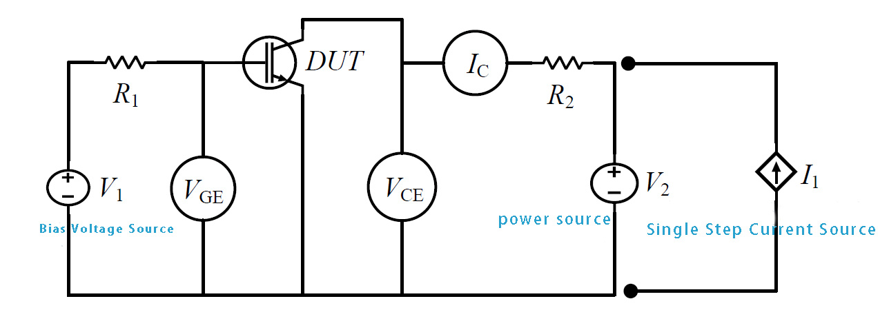
The circuit diagram for testing the saturation voltage parameters of the IGBT module is shown in Figure 1. The specific test process is as follows: first, adjust the voltage of the bias voltage source V1 to the output voltage required in the technical manual of the tested IGBT module. Secondly, when adjusting the voltage source V2, the current value of the ammeter IC should be observed in real time to prevent the current from being too large. When the ammeter IC is displayed as the IC current under the test condition of the saturation voltage parameter in the technical manual of the measured IGBT module, then VCE (sat) is equal to the voltage measured by the voltmeter VCE under the set condition. Among them, R1 should be a large resistance to prevent the IGBT module under test from being broken down due to the excessive bias voltage source V1. When using the pulse method to measure this parameter, the resistance value of the resistor R2 should be selected in combination with the voltage source V2 to prevent the specified collector current from being reached when the voltage source V2 is low enough to ensure that the IGBT module is not broken down. The generation of IC current can also be realized by a single-step current source I1. When I1 outputs current, the resistor R2 should be zero, and the bias condition provided by the bias voltage source V1 remains unchanged.

Figure 1: Saturation voltage test circuit diagram
IGBT Threshold Voltage Testing
The threshold voltage is VGE (th), and th represents the threshold and threshold (Threshold), so it is also called the threshold voltage. The on and off states of the power IGBT module are determined by the gate-emitter voltage VGE (th), and the threshold voltage is required when the IGBT transitions from the off state to the on state or from the on state to the off state The voltage across the gate-emitter. When the voltage across the gate-emitter of the IGBT is greater than this value, the IGBT is turned on; when the voltage across the gate-emitter is less than this value and is a forward voltage, the IGBT is turned off. When the voltage across the gate-emitter is small, the turn-on voltage drop across the IGBT pin CE will become very large, so that the IGBT will easily increase the loss and cause serious heating. As the voltage across the gate-emitter gradually increases, the conduction voltage drop across the IGBT pin CE will gradually decrease, and the losses of the IGBT will also decrease. However, when the voltage across the gate-emitter is too large, the gate of the IGBT will be broken down by the voltage, resulting in the Optimus effect. It is better for the threshold voltage of the IGBT module to be relatively higher. IGBTs are mostly used in places with strong electromagnetic interference. When driving the IGBT, there are more interference signals between the gate and the emitter. When the IGBT is turned off, it must not There is a situation where the interference signal is too large to cause false triggering and cause the device to be turned on. Therefore, the higher the threshold voltage, the better the anti-interference, and the smaller the discrete threshold voltage is, which is also beneficial to the design of the driving circuit. The gate-emitter voltage VGE of a general IGBT module is up to ±20V, and the threshold voltage of the third-generation IGBT is mostly between 5V and 6.5V.
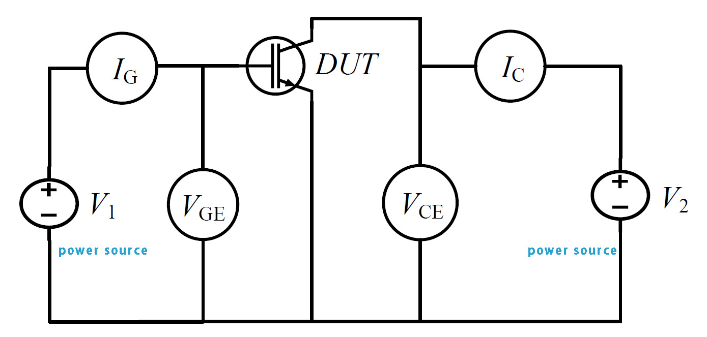
The circuit diagram of the threshold voltage parameter test of the power IGBT module is shown in Figure 2. The specific test process is as follows: first, modulate the voltage source V1 and voltage source V2 to 0V, and connect the power IGBT module under test in the circuit. Jointly adjust the voltage of voltage source V1 and voltage source V2 so that the voltage is 1V lower than the minimum value of the threshold voltage of the measured power IGBT module technical manual, then increase the voltage source V1 and voltage source V2 according to a certain step size, and monitor the ammeter IC in real time When the value displayed by the ammeter reaches the threshold voltage test condition IC of the measured power IGBT module technical manual, then the VGE (th) threshold voltage is equal to the voltage value output by the voltage source V1 under the setting condition of this current value, that is, the voltmeter at this time VGE Measured voltage.

Figure 2 Threshold voltage test circuit diagram
Diode Forward Voltage Testing
Due to its own structural problems, IGBT does not produce parasitic diodes in manufacturing, which is different from the diodes in MOSFETs. However, in order to enhance its reverse withstand voltage value and ensure that the IGBT will not break down the IGBT due to the reverse voltage generated by the sudden shutdown of the high voltage in the presence of an inductive load in some high-power occasions, a continuous IGBT is specially packaged inside. flow diode. From the above introduction, the IGBT loss comes from the common loss inside the transistor and the anti-parallel diode. The loss of anti-parallel diodes comes from two sources: one is the conduction loss generated during forward conduction, that is, freewheeling: Pf; the other is the reverse recovery loss generated during the reverse recovery process: Erec. The conduction loss caused by the forward conduction of the diode is:
𝑃𝑃f = 𝑑𝑑 × 𝑉𝑉F × 𝐼𝐼F (𝑑𝑑: duty cycle during conduction, 𝐼𝐼F: forward current) (2-1)
The conduction loss is related to the diode manufacturing technology and working conditions. The forward conduction voltage VF of the diode is proportional to the passing forward current IF, and increases as the junction temperature Tj of the device increases.
The circuit diagram for testing the diode forward voltage parameters of the power IGBT module is shown in Figure 3. The specific test process is: when measuring the forward voltage of the diode, it is necessary to short-circuit the gate-emitter of the power IGBT module under test to make VGE=0V, so as to prevent the power IGBT from being triggered by false triggering due to interference noise when the gate is suspended. If the module is turned on, it will affect the accuracy of measuring the forward voltage of the diode. When measuring the diode forward voltage of the power IGBT module, there are two measurement methods:
- DC measurement method, by controlling the voltage source V1 to output a DC voltage, or changing the resistance value of the resistor R1 so that the ammeter IC reaches the specified test current value IF and then outputs the current to the device under test. At this time, the value displayed by the voltmeter VCE is Diode forward voltage VF. The measured power IGBT module should reach a state of thermal equilibrium before using the DC measurement method;
- Pulse measurement method, connect the single-step current source to the circuit under test, disconnect the voltage source V1 at this time, set the resistance value R1 to 0Ω or short-circuit it, and adjust the single-step current source to the specified pulse Trigger after the width and pulse amplitude, and the value displayed on the voltmeter VCE at this time is the diode forward voltage VF.

Figure 3 Diode forward voltage test circuit diagram
IGBT Breakdown Voltage Testing
The breakdown voltage is VCES. Most power IGBT modules are made of silicon materials, and the internal structure is a P-N junction and an insulating layer. Due to the IGBT's own characteristics, its ability to withstand voltage and current limit is limited. The so-called breakdown voltage is the withstand voltage value of the pressured IGBT device itself. Once it exceeds this value and is much larger than the withstand voltage value, the IGBT will lose its original Some characteristics lead to the rapid exponential growth of the flowing current, resulting in an unrecoverable avalanche breakdown phenomenon. The breakdown voltage is positively related to the junction temperature Tj, and the higher the temperature, the higher the breakdown voltage of the IGBT. In practical applications, the real breakdown voltage is generally 0.3 times higher than the breakdown voltage rating provided in the IGBT technical manual. The smaller breakdown voltage in the technical manual is to prevent the voltage flowing through the device from being too critical and close to the breakdown voltage, which reduces its own stability and reliability.
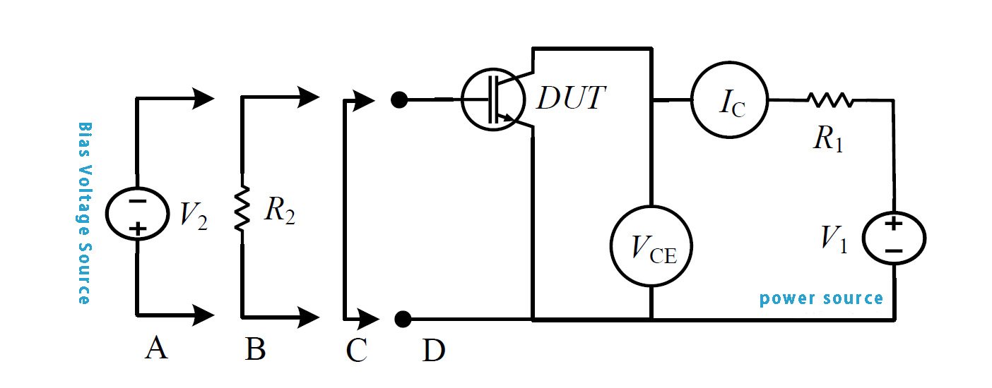
The test circuit diagram of the breakdown voltage parameters of the power IGBT module is shown in Figure 4. The specific test process is as follows: firstly, the corresponding bias conditions A, B, C, and D are respectively applied to the gate-emitter terminals, and the resistor R1 acts as a current-limiting resistor. The output voltage of the collector-emitter voltage source V1 increases in a certain step until it reaches the breakdown voltage under the corresponding bias conditions A, B, C, and D applied between the gate-emitter. During this process, it is detected in real time whether the current value IC of the ammeter is the same as the current value stipulated in the test conditions in the manual. If the current values are the same, the voltage output by the voltage source V1 at this time is the breakdown voltage VCES. The corresponding bias conditions are applied to the gate-emitter terminals respectively. The bias conditions applied respectively are:
A: The gate-emitter applies a reverse bias voltage;
B: Gate-emitter applied resistance circuit;
C: The gate-emitter is short-circuited, VGE=0V;
D: Gate-emitter open circuit.
The four bias modes generally choose mode C to test the breakdown voltage of the power IGBT module. In this mode, the measured value is the breakdown voltage when the IGBT is in a completely off state. The breakdown voltage measured at this time has a higher significance.

Figure 4: Breakdown Voltage Test Circuit Diagram

Nantian Electronics a professional distributor of electronic components, providing a wide range of electronic products, saving you a lot of time, effort and cost through our meticulous order preparation and fast delivery service.
Share this post


